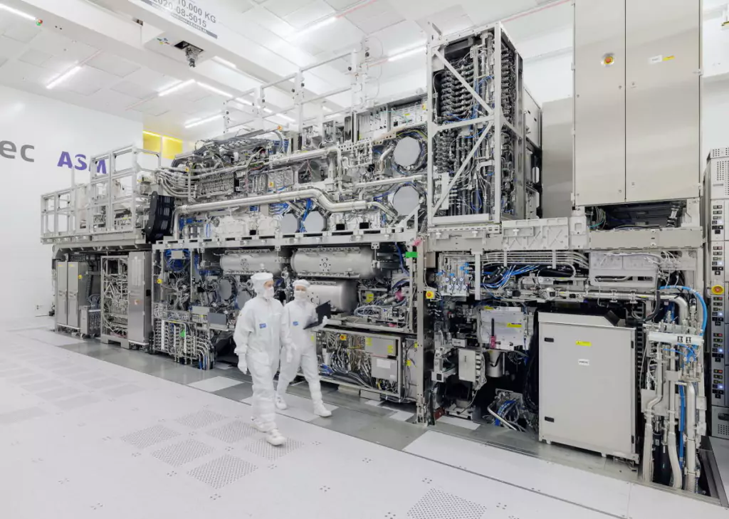
Samsung looks to add its first cutting-edge High-NA EUV lithography equipment by the next quarter, fueling the industry’s semiconductors race.
Samsung Comes Behind Intel & TSMC In Employing High-NA EUV Lithography Equipment, But Competition is Fierce
The utilization of High-NA equipment is now seen as something “premium” for chipmakers, and we recently reported on how Intel managed to acquire five to six kits of ASML’s High-NA Extreme Ultraviolet (EUV) lithography equipment and how it looks like out of the big three semiconductor firms (TSMC, Intel & Samsung), the Korean giant is the last one to receive the next-gen EUV lithography tools from ASML. Based on a report from Sedaily, Samsung expects to receive the equipment either in the next quarter or at the start of 2025, positioning it right along with other semiconductor firms.
The report by the Korean outlet suggests that Samsung is set to receive ASML’s Twinscan EXE:5000 High-NA lithography equipment, which has an 8nm resolution and an EUV light wavelength of 13.5nm. The system will enable chipmakers to produce chips 1.7 times smaller, and transistor densities will see a bump up to 2.9 times. ASML says that the Twinscan EXE:5000 has the industry’s highest productivity, and with the Korean giant getting its hands on the equipment, it’s safe to say that we can expect notable improvements within the firm’s semiconductor ecosystem.

It is said that Samsung plans to set up the first batch of High-NA equipment at the firm’s R&D Hwaseong Campus, but in terms of when we can expect the commercial implementation of the advanced lithography tool, it isn’t certain yet, given that setting up such type of equipment has its own complications, but we can expect the High-NA equipment to come underutilization by the end of 2025, given that Samsung doesn’t face any sort of roadblock in the process.
With Intel, TSMC, and Samsung having access to High-NA, it’s only certain that the semiconductor markets will grow from hereon, and as far as what we are aware of, Intel plans to use High-NA for its 14A node, while TSMC might utilize it in its 2nm class of nodes. For Samsung, this is unconfirmed at the moment, but we expect the Korean giant to follow industry standards, which leads us to believe that the first-generation 2nm process might utilize High-NA.


